REGISTRO DOI: 10.69849/revistaft/ra10202511300711
Julio Hiago de Souza1
Ilmar Duarte dos Reis2
Abstract—Printed Circuit Board Assembly (PCBA) inspection remains a critical step in electronics manufacturing, yet conventional approaches—either purely manual or based on rule-driven Automated Optical Inspection (AOI)—struggle with the increasing miniaturization of SMD components, variable lighting conditions, and the need for rapid adaptation to new product designs. This work introduces an industrial-grade robotic platform that integrates high-resolution imaging, adaptive RGB illumination, robotic actuation, YOLOv8-based defect detection, and photogrammetric 3D reconstruction. The system enables 360° multi-view acquisition through a custom rotation mechanism and provides detailed component-level analysis with high accuracy, outperforming traditional camera-only and commercial smart-sensor approaches. Validated in a smartphone production line in Manaus, Brazil, the platform demonstrates strong robustness, reduced false detections, enhanced traceability through 3D modeling, and a cost–performance ratio suitable for large-scale industrial deployment.
PCBA Inspection, Automated Optical Inspection, YOLOv8, Deep Learning, Photogrammetry, Structure-fromMotion, Robotics, Industrial Automation.
I. INTRODUCTION
Printed circuit board assemblies, or PCBAs, are the foundation of modern electronic systems, especially in highly competitive sectors like consumer electronics and cellular phones. Since failures that go undiscovered can reduce yield, increase return rates, and degrade product quality, inspection processes that can detect even the smallest defects in soldering and componentry are essential to ensuring their dependability. In many industrial units, particularly largescale manufacturing facilities like the Manaus Industrial Pole in Brazil, human operators still play a significant role in PCBA inspection. The physical limitations of human perception and eye fatigue make this approach particularly troublesome for small Surface-Mount Devices (SMDs), leading to components being incorrectly labeled as either acceptable or defective.
Although Automated Optical Inspection (AOI) systems have been used historically as a solution, they continue to encounter difficulties in adjusting to new product designs, detecting miniature SMDs reliably, and preventing false alarms in the presence of changing lighting and positioning [1]. Recent research shows that by utilizing convolutional backbones and feature pyramids to increase robustness in identifying small-scale errors, deep learning architectures can perform noticeably better than conventional methods [2]. Moreover, studies on photogrammetric reconstruction of PCBs show that two-dimensional single-camera examination is frequently inadequate since multi-view data might reveal hidden structures and height changes that are essential for thorough analysis [3].
Standard low-cost existing systems either provide traceability without powerful defect detection or offer partial detection with limited flexibility and exorbitant cost for deployment across many production lines. These shortcomings underscore a glaring technological gap. Inspection technologies that are accurate, economical, and industrially scalable are essential to address this.
Contributions. We introduce an industrial-grade robotic platform for PCBA inspection that combines deep learningbased computer vision, robotic manipulation, and highresolution imaging. The following is a summary of this paper’s primary contributions:
- Robotic inspection platform: A custom-built system capable of rotating the PCB 360° using industrialgrade actuators, ensuring top, bottom, and multi-angle captures.
- High-end imaging and intelligent lighting: Integration of a 20MP macro lens industrial camera with addressable RGB lighting for optimized illumination in defect detection.
- Convolutional Neural Network (CNN)-based inspection: A detection pipeline trained on public and proprietary datasets, capable of identifying and counting miniature SMD components with high accuracy.
- Photogrammetry-based reconstruction: Multi-view geometry is used to create 3D models of inspected boards, allowing for customer traceability and post-production validation.
- Industrial validation: The platform has been implemented in an actual smartphone manufacturing line in Manaus, Brazil, proving its robustness and usefulness in contrast to most approaches that stay at the proof-ofconcept stage.
The remainder of this paper is organized as follows: Section II reviews related work and state-of-the-art inspection techniques. Section III details the proposed system architecture and methodology. Section IV presents experimental results and industrial validation. Section V discusses the broader implications, limitations, and future perspectives. Finally, Section VI concludes the paper.
II. RELATED WORK
A. Automated Optical Inspection and Its Limitations
The popular method for PCB quality assurance has been Automated Optical Inspection (AOI), which aims to either replace or enhance human inspection. Handcrafted rules for lighting, template matching, and tolerance thresholds are a major component of traditional AOI. Although these methods work well for some defect classes, they frequently don’t work well for new product introductions (NPIs) or for accurately detecting tiny SMD components, which are becoming more and more prevalent in consumer electronics. Using lightweight convolutional backbones with dual attention methods can greatly increase robustness when compared to conventional AOI, as shown in [4]. This highlights the transition from solely rule-based pipelines to data-driven approaches.
B. Deep Learning for PCB Defect Detection
Deep learning has dominated PCB defect detection in recent years, and CNN-based architectures are now the industry standard for managing small abnormalities, class imbalance, and changeable lighting. Specifically, Yao et al. [5] suggested an improved YOLOv8 variation (IEMAYOLOv8) designed for PCB defect detection, showing decreased false detections and increased accuracy on small components. Complementary methods, like dataset-specific adaptations and data augmentation, concentrate on training efficiency and generalization [6], [7]. The importance of using contemporary object detection backbones for industrial inspection jobs is highlighted by these contributions.
C. Three-Dimensional Inspection and Photogrammetry
A number of studies have investigated the use of 3D reconstruction in PCB inspection in addition to traditional 2D imaging. In their investigation of camera-based rectification techniques for reconstructing PCB height profiles, Breier et al. [3] showed that multi-view geometry can capture structural information that is not available for singlecamera examination. Robust procedures for recovering camera poses and dense point clouds from unordered image sequences have been built using more general frameworks like COLMAP, which is based on Structure-from-Motion (SfM) and Multi-View Stereo (MVS) [8]. These techniques are being used more and more in industrial settings to give geometric traceability to visual examination.
Although X-ray and CT-based modalities are still viable options for volumetric inspection, mass production lines cannot use them due to their high cost and limited inline scalability. A non-destructive and economical method is provided by camera-based photogrammetry, especially when combined with robotic manipulation to guarantee full 360◦ board coverage. But without being integrated into an industrial inspection platform, previous research has usually concentrated on either algorithmic reconstruction or lab-scale validation. Because of this gap, photogrammetric modeling is incorporated into our suggested solution to meet the objectives of client validation and defect traceability.
D. Positioning of This Work
In conclusion, earlier studies show distinct advancements in deep learning-based PCB flaw identification, expanding inspection to 3D geometry, and fusing robots and vision systems. The majority of submissions, however, either concentrate on incomplete elements like 3D modeling without integration into defect detection pipelines [3] or are restricted to algorithmic proposals without industrial deployment [5], [4]. The industrial-grade robotic platform we present fills these gaps by combining: (i) intelligent lighting and highresolution macro-imaging; (ii) defect detection based on YOLOv8 that is specific to SMD-scale components; (iii) photogrammetric reconstruction for post-production traceability; and (iv) validation in an actual smartphone manufacturing environment.
III. SYSTEM ARCHITECTURE AND METHODOLOGY
The presented platform combines mechanical manipulation, high-resolution imaging, deep learning-based fault identification, and photogrammetric reconstruction into an end-to-end inspection cell. Mechanical and electronic subsystems, control and actuation, computer vision and YOLOv8based flaw detection, and photogrammetry and server integration comprise the system’s four primary levels. Fig. 1 shows the workflow and Fig. 2 shows the final device.

Fig. 1. Flowchart of the proposed PCB inspection system, showing sequential stages from PCB input to final visualization.
A. Mechanical and Electronic Subsystem
The operator can easily access the interior chamber thanks to the inspection device’s robust yet lightweight design, which was made utilizing 3D printing (ABS and PETG). The PCB is positioned using a retractable tray with alignment guides for examination. Following detection, a high-precision rotary actuator (Steadywin GIM4310-10 with 1:10 reduction, CANbus communication) rotates the PCB 360◦ while a servo-driven clamp (Feetech STS3095, 100 kg torque) secures it. An EMAX ES08MDII secondary servo powers the tray retraction mechanism. The Fig. 3 shows the initial design for the platform development made at OpenAI Sora Model image generator.

Fig. 2. Actual Final Version of the Device Implemented in Industry.

Fig. 3. Inicial device conecpt render and sketch
The illumination is provided by addressable RGB LEDs (WS2812 family), which enable adaptive lighting modes (white for capture, yellow for indexing, blue for standby, and green/red for acceptance/rejection). The custom PCB control board, as shown in Fig. 5, which is responsible for LED status control and actuator coordination, is built on top of the Atmega328p-pu microcontroller. A current sensing circuit monitors clamp torque to prevent mechanical stress in sensitive areas, such as the golden fingers. Fig. 4 shows the different colors that the device assumes to show the operation of the equipment to the user.
B. Control and Actuation Layer
All actuators, illumination conditions, and synchronization with the high-resolution imaging procedure are managed by the control layer. The Python 3.8 implementation manages high-level sequencing and uses UART to connect to the custom Atmega328p-based controller. Low-level operations

Fig. 4. RGB Lighting System

Fig. 5. RGB Lighting System
like PWM generation for servomotors and clamping unit current monitoring are carried out by this controller.
A finite state machine (FSM) governs the inspection sequence, ensuring deterministic operation and operator safety. The states and transitions are defined as follows:
- Standby: The system remains idle with blue illumination, signaling readiness for a new inspection cycle.
- Indexing: A lightweight CNN model (trained with Google Teachable Machine and deployed via TensorFlow Lite) continuously analyzes the camera feed to detect PCB presence in the tray. Upon detection, yellow illumination alerts the operator of imminent indexing.
- Clamping: The tray is retracted using a reinforced SG90 servo, while the Feetech STS3095 (100 kg torque) clamp secures the PCB. A current-sensing module monitors torque to prevent over-compression, protecting sensitive features such as golden fingers Fig. 6.
- Capture: The WS2812 RGB LED array switches to high-intensity white mode, ensuring uniform illumination. The Steadywin GIM4310-10 actuator rotates the PCB a full 360◦ at a constant angular velocity (Fig. 7). During this rotation, the industrial camera (HT-SUA2000C-T, 20 MP, 24 mm f/1.8 macro lens) continuously acquires a multi-view image sequence. From this process, three distinct outputs are produced: (i) a high-resolution top view, (ii) a bottom view, and (iii) a dense sequence of side-angle images to be later used in photogrammetric 3D reconstruction.
- Completion: After the full rotation, the tray returns to its initial position. Captured data are transferred to the vision module, which performs preprocessing, YOLOv8 inference, and subsequent 3D reconstruction.

Fig. 6. Adjustable Clamp System

Fig. 7. Smooth Rotation System
Actuation and imaging are guaranteed to stay closely synced thanks to this architecture. The system accomplishes resilience and modularity by separating low-level control (embedded microcontroller) from high-level sequencing (Python). Additionally, without affecting real-time limitations, the FSM-based design enables the simple extension of new states (such as error handling and retest loops).
C. Computer Vision and YOLOv8-based Defect Detection
The YOLOv8 object identification framework, which has been modified for PCB assembly inspection with a focus on tiny SMD components, is utilized by the vision module. The backbone network uses depthwise convolutions and a CSPbased design, which allows for a good trade-off between inference speed and detection accuracy. Weights pre-trained on publicly available PCB defect datasets were used to initialize the model at first [6], [7]. These weights provided baseline representations for solder bridges, missing components, and pad misalignments. Following that, 1,440 proprietary high-resolution photos taken on the client’s production line—which included both defective and non-defective SMD cases—were used for fine-tuning. A Roboflow-inspired internal graphical interface was used to annotate the dataset, allowing for accurate polygonal component labeling.
A number of data augmentation techniques, including random rotations (±15◦), brightness and contrast jittering, Gaussian noise injection, and synthetic occlusion, were used to improve robustness in real-world industrial settings. These enhancements lessen the performance deterioration brought on by changing lighting and camera angles. An NVIDIA RTX-class GPU (12 GB VRAM), a batch size of 16, input resolution of 640×640 pixels, and an AdamW (PyTorch Library Weight Optimizer Algorithm) optimizer operating at a learning rate of 1×10⁻⁴ were all used in the training process. After 100 epochs, early stopping was used, which produced stable convergence free of overfitting.
A digital enhancement pipeline comprising histogram equalization, adaptive contrast boosting, unsharp masking, and non-local means denoising is used to preprocess the top and bottom PCB pictures before inference. Before CNN processing, these actions enhance fine-pitch component feature visibility. For every component that is recognized, YOLOv8 produces bounding boxes and class labels together with positional data, confidence ratings, and the likelihood of a defect specific to a given class. Counts and the predicted bill of materials (BOM) reference are automatically crossvalidated, and any differences are marked as potential flaws.
Fig. 8 shows the outcome of a representative inference. An open-source Arduino Pro Micro board is used as a standin PCB in the example for secrecy reasons; the real client smartphone PCB cannot be shown. Bounding boxes in this picture indicate detected headers, passive components, and ICs, illustrating the model’s great precision in identifying small-scale constituents.

Fig. 8. Comparison between original PCB photo and YOLOv8 component prediction
D. Photogrammetry and 3D Reconstruction
The inspection platform uses a photogrammetric processing in addition to 2D photography to improve contextual visualization and defect tracking. The COLMAP framework [8], which integrates Structure-from-Motion (SfM) and Multi-View Stereo (MVS) methods, is used to process the rotating picture sequence obtained during the capture phase. MVS densifies the reconstruction into a high-resolution 3D point cloud, whereas SfM uses feature correspondences throughout the multi-view dataset to estimate camera positions. After that, a textured mesh is created, which makes it possible to see the PCB topology and component placement in depth.
There are two main benefits to this 3D reconstruction. By enabling operators and quality engineers to reexamine damaged boards with geometric context, it first improves defect tracing and reduces disagreements in warranty or production yield talks. Customers can interactively examine the reconstructed PCB model through the server-client interface, providing an easy-to-use medium for remote validation.
Although X-ray and CT-based 3D inspection methods are still well-established substitutes for multilayer PCBAs, they have limitations in terms of inline scalability, high equipment costs, and radiation shielding needs. Camera-based multiview reconstruction, on the other hand, provides an affordable and non-destructive approach that easily complements current optical inspection procedures [3]. Photogrammetry has enough spatial fidelity to confirm surface-mounted components and board bending, despite the fact that it cannot detect internal solder joints or buried vias.
For demonstration purposes, Fig. 9 illustrates a representative reconstruction with the standard quality of this model type.
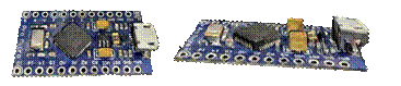
Fig. 9. 3D Model COLMAP Reconstruction
E. Server Integration and User Interface
Immediately following each cycle, all inspection findings are sent to a local server architecture to facilitate historical traceability and real-time monitoring. The communication layer uses a RESTful Python API (FastAPI) that receives binary payloads with top/bottom photos, YOLOv8 detection overlays, and 3D reconstruction files in PLY/OBJ format in addition to JSON-formatted metadata. The Pyzbar package is used to extract the unique DataMatrix serial code from each PCB during capture, which serves as an index. This guarantees clear mapping between the manufacturing line’s physical units and the digital data that relate to them.
Utilizing PostgreSQL for structured storage of inspection logs, component counts, and defect annotations, as well as asynchronous endpoints for concurrent uploads, the backend architecture is built for scalability. Large production batches may be efficiently retrieved thanks to the storage of image and 3D assets in a specialized object repository. Because of the system’s capability for role-based access control, managers, operators, and quality engineers can query results based on their privileges.
ReactJS is used to construct the client-facing interface, which is intended to render big image datasets with minimal delay. There are four synchronized panels on the web dashboard: YOLOv8-annotated overlays with identified components and flaws, (i) the original top-view image, (ii) the original bottom-view image, and (iv) an interactive Three.jsbased 3D viewer for traversing the rebuilt mesh. Cross-panel synchronization improves defect validation and decisionmaking during rework or rejection by allowing operators to connect 2D detections with 3D geometry.
In addition to providing inline operators with instant feedback, this server integration aggregates data over time for yield analysis. Defect frequency, component misplacement trends, and process drift are examples of aggregated statistics that can be transmitted to enterprise resource planning (ERP) platforms or higher-level manufacturing execution systems (MES).
Fig. 10 shows a representative photo of the user interface (PCB censored for confidentiality purposes)
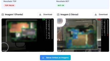
Fig. 10. User Interface Visualization Example
F. Summary of Innovations
The methodology introduces a tightly integrated workflow that combines:
- High-resolution imaging with adaptive RGB lighting.
- Robotic manipulation for 360◦ PCB coverage.
- YOLOv8-based defect detection optimized for SMD components [5].
- Photogrammetric 3D reconstruction for enhanced traceability.
- Industrial validation in a smartphone PCB production line.
This integration directly addresses the shortcomings of prior AOI systems [4] and complements existing research on PCB photogrammetry [3].
IV. EXPERIMENTS AND INDUSTRIAL VALIDATION
A. Experimental Setup
Three inspection strategies were compared:
- Baseline camera: A consumer-grade digital camera (400–800 BRL, ∼80–160 USD), providing only topview images without automated defect detection.
- Keyence IV3 sensor: A commercial smart camera solution (28,000 BRL, ∼5,600 USD in the Brazilian market), capable of simple classification and assembly error detection.
- Proposed robotic platform: The developed inspection system (8,000 BRL, ∼1,600 USD total cost), integrating a high-resolution industrial camera, robotic rotation stage, and YOLOv8-based defect detection with photogrammetric reconstruction.
B. Quantitative Results
The evaluation considered both the performance of the defect detection model and the overall efficiency of the inspection platforms. Table I reports the quantitative results of YOLOv8 on the proprietary dataset, using 1,440 annotated PCB images collected from the production line. Metrics include precision, recall, F1-score, and mean Average Precision (mAP) at both IoU 0.5 and IoU 0.5:0.95. Results demonstrate that the model achieves high accuracy in detecting miniature SMD components across both top and bottom views.
TABLE I
YOLOV8 DETECTION PERFORMANCE ON PROPRIETARY PCB DATASET

The primary performance and cost indicators for the three examined systems (baseline camera, Keyence IV3, and the proposed system) are compiled in Table II together with the vision model metrics. After evaluating the suggested platform’s cycle time across 300 boards, an average of 4.625 seconds per inspection was found.
TABLE II
COMPARISON OF INSPECTION APPROACHES

C. Discussion of Results
Despite its low cost and quick capture time, the baseline camera was unable to detect defects and only produced static images, making it unsuitable for industrial application. Despite being quicker than the suggested platform, the Keyence IV3’s limited image resolution and locked, non-trainable AI engine made it difficult to identify tiny SMD components, especially those with a footprint smaller than 0402. Furthermore, large-scale deployment in the Brazilian market is not economically possible due to its high acquisition cost (28,000 BRL per unit).
The suggested robotic platform, on the other hand, offers better defect detection with YOLOv8, with the capacity to consistently categorize and count tiny components across the board, even though its cycle time is marginally longer (average 4.625 s). Multi-view photogrammetric reconstruction improves traceability even more by offering 3D visual proof for resolving disputes. The platform, which costs 8,000 BRL in total, strikes the ideal combination between price, scalability, and precision, allowing it to be implemented across several manufacturing lines.
REFERENCES
[1] Q. Ling and N. A. M. Isa, “Printed circuit board defect detection methods based on image processing, machine learning and deep learning: A survey,” IEEE Access, vol. 11, pp. 15921–15944, 2023.
[2] Z. Hu and Y. Wang, “Detection of PCB surface defects with improved faster R-CNN and feature pyramid network,” IEEE Access, vol. 8, pp. 108335–108345, 2020.
[3] M. Breier, P. Kusters, A. K¨ onig, and W. Li, “Rectification for fronto-¨ parallel camera movement in 3d reconstruction of printed circuit boards,” in 2016 IEEE International Symposium on Industrial Electronics (ISIE), 2016, pp. 625–630.
[4] L. Wu, L. Zhang, and Q. Zhou, “Printed circuit board quality detection method integrating lightweight network and dual attention mechanism,” IEEE Access, vol. 10, pp. 87617–87629, 2022.
[5] L. Yao, B. Zhao, X. Wang, S. Mei, and Y. Chi, “A detection algorithm for surface defects of printed circuit board based on improved yolov8,” IEEE Access, vol. 12, pp. 118234–118246, 2024.
[6] I. Bhattacharya, N. Honrao, S. Ghosal, and A. Basu, “End-to-end deep learning framework for printed circuit board manufacturing defect classification,” Scientific Reports, vol. 12, no. 1, p. 12559, 2022.
[7] P. Klco, D. Koniar, L. Hargas, K. P. Dimova, and M. Chnapko, “Quality inspection of specific electronic boards by deep neural networks,” Scientific Reports, vol. 13, p. 20657, 2023.
[8] J. L. Schonberger and J. M. Frahm, “Structure-from-motion revisited,”¨ in Proc. IEEE Conference on Computer Vision and Pattern Recognition (CVPR), 2016, pp. 4104–4113.
1 juliosouzasw@gmail.com
Grad. Engenharia Elétrica
2 ilmardr@yahoo.com.br
M.Sc Engenharia de Produção